Introduction
The purpose of this project is to build a simple Arithmetic Logic Unit (ALU) with a 4-bit word size on a DE10-Lite board with a Max 10 10M50DAF484C7G FPGA. This ALU interfaces with external LEDs, 7-segment displays, buttons, and switches and was developed using behavioral Verilog specifications in the Quartus development environment. The operations of this ALU are broken into 3 modes: a Logical mode, an Arithmetic mode, and a Comparison mode. The Logical mode includes bitwise AND, OR, and XOR operations for two 4-bit numbers and a NOT operation for an 8-bit number. The Arithmetic mode includes 4-bit addition and subtraction, and 8-bit multiplication and division by 2. The Comparison mode includes greater than, less than, and equality comparisons of two 4-bit numbers as well as an operation to determine the maximum value of two 4-bit numbers.
A block diagram depicting the top module of the ALU can be seen below in Figure 1. As seen in this diagram, the switches (SW 0-9) and buttons (KEY 0-1) are inputs to the FPGA, and the LEDs (LED 0-9) and seven segment displays (HEX 0-1) are outputs. SW 0-7 act as the binary inputs for the two 4-bit numbers or the one 8-bit number that is to be operated on by the ALU. SW 8-9 act as the select bits to the operation multiplexers that control the flow of data out of the logical, arithmetic, and comparison modules. The KEY 0-1 buttons are the select bits to the mode multiplexer that controls the data path to the seven-segment display and LEDs. By pressing the buttons KEY0 and KEY1 and flipping the switches SW8 and SW9 on the DE10-Lite board, the user can control the result that is output to the LEDs and seven segment displays. The binary encoding of these bits is shown in the truth table in Figure 2.
The seven-segment display produces a hexadecimal representation of the operation result using a 4-to-8 binary decoder, and the LEDs display the corresponding binary representation. Since two hex displays are used for displaying the result in this project, the ALU is limited to representing numbers only up to 8 bits. Two more seven segments displays (HEX 4-5) are used to display the state of the select bits for the mode multiplexer. Since this multiplexer is implemented using button inputs, it is otherwise difficult to keep track of the current mode.

Figure 1: Block diagram of the Verilog design for the Arithmetic Logic Unit. Includes the top module (Project1_top) and the key sub modules (Comparison, Logical, Arithmetic, Operation Select Mux, Mode Select Mux, and Seven Segment)
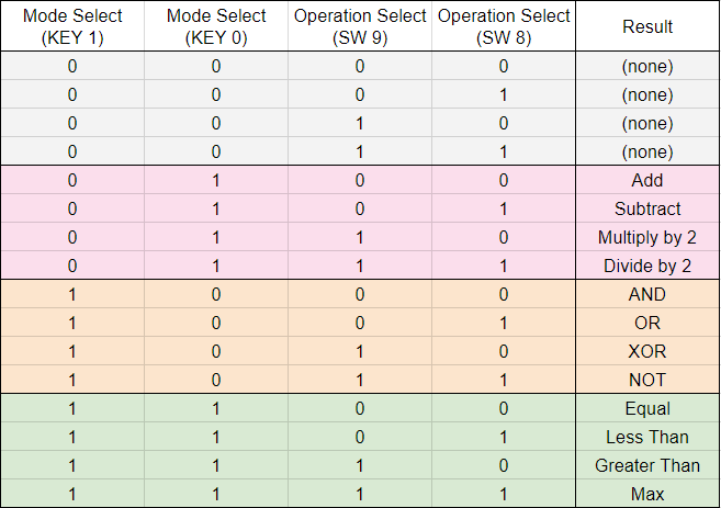
Figure 2: Mode Select and Operation Select Multiplexer Truth Table. These multiplexers were implemented using procedural case statements. Table is color coded according to the block diagram above.
Arithmetic Mode
The 4-bit addition and subtraction modules of the Arithmetic mode operate using a Ripple-Carry adder and Ripple-Borrow subtractor implementation derived from the truth tables in Figure 3 and 4. To add two 4-bit numbers, the adder module connects 4 full adder circuits in parallel. The carry input to the first full adder, C_in, is grounded since the first two bits of the addition will never have a carry. The same procedure applies for the subtraction module, which combines 4 full subtractors and grounds the first borrow input, B_in. If a carry is produced in either the adder or the subtractor, it is concatenated on to the sum before exiting the module so that the correct number is always represented, even if it exceeds 4 bits. Since the addition or subtraction of two 4-bit numbers will never exceed 8 bits, it is not necessary to check for overflow.

Figure 3: Full Adder truth table. X and Y are the numbers to be added, C_in is the carry in, C_out is the carry out, and S is the sum
|

Figure 4: Full Subtractor truth table. X and Y are the numbers to be subtracted, B_in is the borrow in, B_out is the borrow out, and D is the difference
|
Given the truth tables in Figure 3 and 4, and the similarities in implementation for the full adder and full subtractor, it is clear to see that a Ripple Carry adder and Ripple Borrow subtractor circuit are nearly identical. In fact, by inverting one of the input numbers and setting the C_in high on a Ripple Carry adder, the 2’s compliment of the number is produced. Therefore, it is important to note that by adding one number and the other number’s 2’s compliment, it is possible for an adder to perform subtraction as well. To demonstrate this concept, however, the adder and subtractor circuits are left as independent modules in the implementation for this project.

Figure 5: Addition result of x + y where x = 0xA = 0b1010 and y = 0x7 = 0b0111. Result is displayed in hex by the seven segment display as 0x11 and displayed in binary by the LEDs as 0b0001_0001.
|
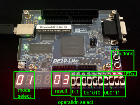
Figure 6: Subtraction result of x - y where x = 0xA = 0b1010 and y = 0x7 = 0b0111. Result is displayed in hex by the seven segment display as 0x03 and displayed in binary by the LEDs as 0b0011.
|
Multiplication by 2 and division by 2 is most efficiently completed by bitwise shifting, which can be done in Verilog using the shift operator. Since the ALU can only represent numbers up to 8 bits, and the multiplication module takes in an 8-bit number, it is necessary to check for overflow. To do so, the division module records the value of the least significant bit before shifting the bits one place to the right and the multiplication module records the value of the most significant bit before shifting the bits one place to the left. If this recorded carry bit is 1 for either the multiplication or division, there will be overflow. If there is overflow, LED 9 and the decimal point on the seven-segment display will turn on when displaying the result. An example of his can be seen in Figure 7 and 8, where both operations produce overflow. If there is overflow, the actual result for a number multiplied by 2 will be 256 plus the number displayed, and the actual result for a number divided by 2 will be the number displayed plus 0.5.

Figure 7: Multiplication result of 2*{x, y} where x = 0xA = 0b1010 and y = 0x7 = 0b0111. Result is displayed in hex by the seven segment display as 0x4E. and displayed in binary by the LEDs as 0b0001_0100_1110. The decimal point on the seven segment display and the 9th LED (second LED from the left) is turned on to signify overflow. The actual result in base 10 is 256 + 0x4E = 256 + 78 = 334.
|

Figure 8: Division result of {x, y}/2 where x = 0xA = 0b1010 and y = 0x7 = 0b0111. Result is displayed in hex by the seven segment display as 0x53. and displayed in binary by the LEDs as 0b0001_0101_1100. The decimal point on the seven segment display and the 9th LED (second LED from the left) is turned on to signify overflow. The actual result in base 10 is 0x53 + 0.5 = 83 + .5 = 83.5.
|
Logical Mode
The Logical mode computes bitwise AND, OR, and XOR of two 4-bit numbers and bitwise NOT of an 8-bit number. These modules were designed using continuous assignment and behavioral gate representations. Example output of these operations can be seen in Figures 9-12 where the 4-bit numbers x and y are equal to 0xA and 0x7 respectively.

Figure 9: Logical result of x & y where x = 0xA = 0b1010 and y = 0x7 = 0b0111. Result is displayed in hex by the seven segment display as 0x02 and displayed in binary by the LEDs as 0b0010.

Figure 11: Logical result of x ^ y where x = 0xA = 0b1010 and y = 0x7 = 0b0111. Result is displayed in hex by the seven segment display as 0x0D and displayed in binary by the LEDs as 0b1101.
|

Figure 10: Logical result of x | y where x = 0xA = 0b1010 and y = 0x7 = 0b0111. Result is displayed in hex by the seven segment display as 0x0F and displayed in binary by the LEDs as 0b1111.

Figure 12: Logical result of ~{x, y} where x = 0xA = 0b1010 and y = 0x7 = 0b0111. Result is displayed in hex by the seven segment display as 0x58 and displayed in binary by the LEDs as 0b0101_1000.
|
Comparison Mode
The equal, greater than, and less than comparisons were implemented using procedural statements with an always block and the greater than, less than, and equal to operators in Verilog. The max comparison was implemented using continuous assignment with the logical expression obtained from the truth table seen in Figure 13.
To obtain the truth table for the max operation, the maximum value between X and Y was evaluated at every value of X and every value of Y. Since in many cases, the maximum value can be determined solely by evaluating the position of the most significant 1 for both numbers, the presence of many “don’t cares” in the truth table dramatically simplifies the result. For example, if X is equal to 0b0100 and Y is equal to 0b0011, it is clear that X is larger, simply by looking at the third bit of each number since the third bit of X is a 1 and the third bit of Y is a 0. Any combination of the first two bits of Y cannot exceed the magnitude of X. Thus, in this scenario, the first two bits of both X and Y can be treated as “don’t cares.” The Sum of Products logical expression for this truth table can then be obtained by considering all Y’s to be 1 and all X’s and X+Y’s to be 0. Thus, if this logical expression evaluates to be true, it means that Y is the max, and vice versa. Figures 14-17 show an example output of each operation in the Comparison mode.
To obtain the truth table for the max operation, the maximum value between X and Y was evaluated at every value of X and every value of Y. Since in many cases, the maximum value can be determined solely by evaluating the position of the most significant 1 for both numbers, the presence of many “don’t cares” in the truth table dramatically simplifies the result. For example, if X is equal to 0b0100 and Y is equal to 0b0011, it is clear that X is larger, simply by looking at the third bit of each number since the third bit of X is a 1 and the third bit of Y is a 0. Any combination of the first two bits of Y cannot exceed the magnitude of X. Thus, in this scenario, the first two bits of both X and Y can be treated as “don’t cares.” The Sum of Products logical expression for this truth table can then be obtained by considering all Y’s to be 1 and all X’s and X+Y’s to be 0. Thus, if this logical expression evaluates to be true, it means that Y is the max, and vice versa. Figures 14-17 show an example output of each operation in the Comparison mode.

Figure 13: Truth table for max operation with two 4-bit numbers

Figure 14: Comparison result for x == y where x = 0x8 = 0b1000 and y = 0x7 = 0b0111. Result is displayed in hex by the seven segment display as 0x00 and displayed in binary by the LEDs as 0b0000.
|

Figure 15: Comparison result for x < y where x = 0x8 = 0b1000 and y = 0x7 = 0b0111. Result is displayed in hex by the seven segment display as 0x00 and displayed in binary by the LEDs as 0b0000.
|

Figure 16: Comparison result for x > y where x = 0x8 = 0b1000 and y = 0x7 = 0b0111. Result is displayed in hex by the seven segment display as 0x01 and displayed in binary by the LEDs as 0b0001.
|
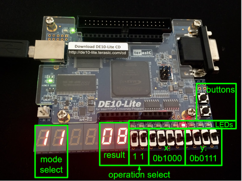
Figure 17: Comparison result for max(x, y) where x = 0x8 = 0b1000 and y = 0x7 = 0b0111. Result is displayed in hex by the seven segment display as 0x08 and displayed in binary by the LEDs as 0b1000.
|
Seven Segment Display
In order to display the operation result in hexadecimal on the seven segment display, the result must pass through a 4-to-8 decoder. This decoder was implemented using procedural if statements and case statements in Verilog according to the truth table in Figure 18 below, which maps every 4-bit number to the corresponding representation of that number in hexadecimal on the display. If the number to be displayed has a carry bit of 1, then overflow is present, and the decoder will turn on the decimal point on the display as well.

Figure 18: Truth table for the seven segment display decoder (without the decimal point)
Conclusion
This project was a very effective introduction into learning the basics of Verilog. Since Verilog requires that the design follows the rigid structure of modules and sub-modules, this project was a great example of why it is important to plan out a design plan and block diagram before beginning to write code. The most difficult part of this project was getting accustomed to the Quartus environment. Since I had never worked with Quartus before, it required a lot of overhead work simply to understand how the environment worked, learn how to run and compile my code, and ensure that my pin planning was correct, but it was good experience to be able work through it and figure it out on my own. I also learned many lessons from repetitive mistakes I made along the way. One such lesson is to always be as explicit as possible in my code (i.e. declaring all wires and their widths, declaring sensitivity lists, etc) so that there is no confusion as to what the compiler interprets versus what I am trying to do. These can be difficult bugs to find, so it is a good idea make the effort to avoid them altogether.
